TapNLink User Manual
Introduction
This documentation covers details that are not covered in the Getting started.
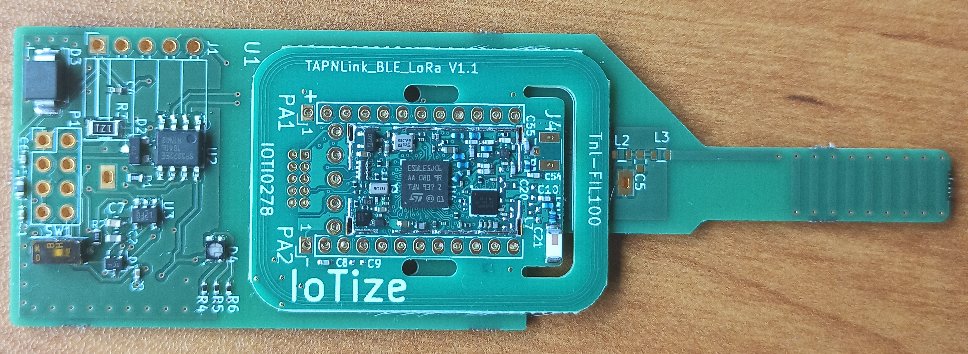
Electrical connections
This section describes the electrical interface for following TapNLink modules: TnL-FIR103, TnL-FIW103 & TnL-FIT203.
Mechanical connections
This section describes how to physically connect the TapNLink to the target.
Direct soldering of TapNLink modules on PCB
TapNLink modules can be soldered automatically onto a PCB:
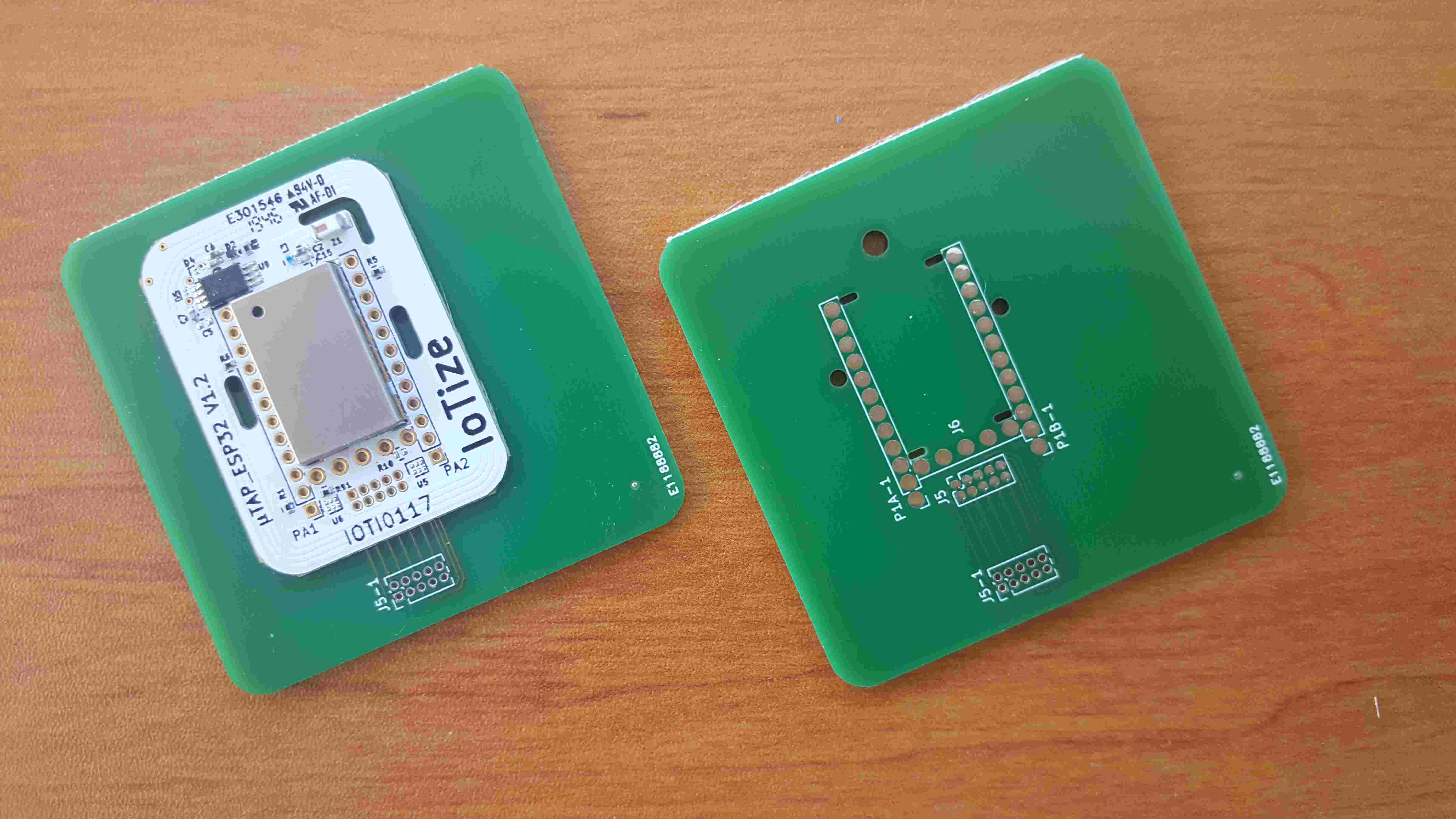
This technique is cost effective but precautions are required:
- the NFC antenna must be kept far away from metallic areas,
- milling must be done to make room for the 4 pins of the shield (for WiFi and BLE modules), so that the TapNLink is flush with the PCB,
- traces should be routed between Tap and the PCB (the PCB conformal coating is not an insulator),
- vias can safely be made just outside the P1A.1-12 and P1B.1-12 pins, so traces can be routed safely to the outside layer (near the black lines).
- paste must be applied to approx 80% of the SMD pads, so that excess paste goes directly into the Taps pin holes, and not onto the PCB.
Do not hesitate to contact IoTize to receive detailed information about this technique.
I/O pins
These are made use of by Java so are described in the Java documentation.
Factory reset
This section describes how to perform a factory reset and recover IoTize default configuration.
Configuration
You define the way TapNLink communicates with the target system in IoTize Studio, as described in Part II of the appropriate Getting started.
Create App
You then create your App.